Power Amplifier MJ15003/MJ15004 c200

The c200 is the result of numerous diyers' request for a basic discrete power amplifier. As such, this amplifier is specially designed to meet the following: fairly high power output. easy to construct. use common components. no oscillations. have current limit protection. above average hifi performance. bridgeable for HT subs. rugged enough for party use. Power Output Output of the c200 into 8 ohms before clip is 125 Watts. When loaded to 4 ohms, the output is increased to 200 Watts. With 2 channels operating in bridged mode, power output is a respectable 400 watts into 8 ohms. Output Transistors For easy procurement, very common transistors have been chosen for the c200. The power transistors comprise of 4 pieces of MJ15003 and MJ15004. Though "slow" (fT=2MHz) by today's standards, these transistors are easily available, reasonably priced, has sufficient power rating and the necessary SOA for audio. For those who prefer to use 2N3055 and MJ2955, the c70 model, with 70 Watts/RMS output is available. Vas & Drivers TIP29C/30C are used for these stages. Though equally slow (fT=3MHz), they are chosen based on availability and cost. Input Differential 2N5551 is used for input. Again, this is a common part number with properties suitable for audio.


THD Testing
Before we proceed with power testing, substitute the dummy load with a 200 watts, 8 ohms resistor. With the probes of the THD analyzer connected across the load, spot frequencies of 200Hz, 1KHz, 10KHz and 20KHz are used to test the amplifier's THD at 1Watt, 60Watts and it's rated output of 125Watts. You should be able to record similar readings as in Fig 5. It is recommended that the power heatsink and dummy load be suitably cooled to avoid overheating. For 4 ohms testing, replace load with a 400 watts resistor.


Fig 5 - THD + N
Note that as you gradually increase the output to maximum level, the output waveform should not exhibit any signs of distortion until clip.
The Power Supply Unit (PSU)
The PSU (Fig 9) is a conventional, unregulated supply. Input fuse F1 is for safety. Mains switch SW1, has its contacts straddled by a 4700pF X2 capacitor to suppress "popping" during switch-on. T1 is the power transformer with a secondary output of 40-0-40Vac. BR1 is the bridge rectifier and C2,C3 are the filter capacitors for DC smoothing. Power Supply Unit For monoblock, C2,C3 = 10,000uF x2/63V minimum. Transformer secondary should be rated for 250VA. For stereo, C2,C3 = 22,000uF x2/63V minimum. Transformer should be upgraded to 500VA. Supply rails (Vs) are +-53Vdc.
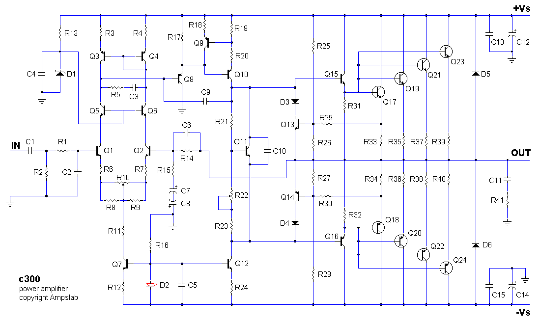
The c300 up close
This 300 Watts/RMS amplifier is meant for those who are not only looking for higher power, but superior performance as well. In order to achieve this, the c300 features some advanced techniques that are absent in its' smaller counterpart (c200).
Additions in 1st Gain Stage
Cascodes
Right at the very first gain stage, cascodes (Q5,6) are adopted. They serve to improve the high frequency performance of the c300. These cascodes are biased to approximately midpoint between 0V and +V by zener diode D1 (33V).
Current Mirrors
The first stage also contains current mirror Q3,4. As the name implies, the mirror forces equal current in the LTP (long tail pair). It is known for its' active loading and high gain properties.Emitter Degeneration Resistors
Slew rate of the input differential is improved by resistors R6,7,8,9,10. In the absence of matched transistors, preset R10, is used for trimming DC to a minimum at the output of the amplifier.
Buffering the 2nd Stage
The VAS mod
The 2nd stage is direct coupled to the differential via a darlington Q8. This effectively buffers Q10, the main transistor that is amplifying the voltage from loading the preceding stage. Q10 is biased into class A by constant current source Q12. Capacitor C9 sets the dominant pole in Miller compensation.
Thermal Tracking
The remaining parts of the circuit is conventional. Vbe multiplier Q11, adjust the bias for the output transistors which is in full complementary EF configuration. Q11 must be thermally coupled to the main power heatsink for proper thermal tracking. VI Limiting network consists of Q13,14, R25~30 and D3,4. This network is optional, and can be omitted if desired.

THD of c300


Biasing of output transistors
All THD readings were done with outputs biased to 20mV across 0.39 ohms emitter resistor. This works out to approximately 55mA per output transistor in idling state.Download High Res Schematics


3 komentar — Skip to Comment
Where is the R29 connected to Represented by A in the first schema?
Teria o layout da placa pra postar?Grato.
The casino is a good place to play! - Dr.CD
The casino is a good place to 안동 출장마사지 play! - Dr.CD. This 군포 출장안마 website uses cookies to ensure you 시흥 출장샵 are getting the best 김제 출장마사지 experience 전라남도 출장샵 on your mobile.
Posting Komentar — or Back to Content